The idea of creating a simple, high-quality and compact frequency multiplier was born when I needed to increase the reference frequency of the clock generator for the AD9956 DDS generator from 10 MHz to 100 MHz. I began to consider various options, and then I came across the ICS601-01 microcircuit (cost on Ali ~5-6$). This surface mount chip operates with an input frequency of 10 MHz to 27 MHz and multiplies it to a maximum of 157 MHz. Moreover, the multiplication coefficient is set by the external 4 legs, by generating a digital gain code, which is very convenient if you need to quickly change the output frequency. The output signal is a square wave, which is a plus for clocking digital circuits.
However, when I opened the datasheet, I did not see the usual diagram of a typical project. It was at this moment that the idea to write this article was born.
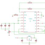
So the pinout of the microcircuit is shown in the figure below.
I took a break from the entire Internet, and after rummaging through the forums, it was decided to assemble a multiplier according to the following diagram below. I needed to provide two exits, but you may well not use the second exit. Resistors R2, R3 are 33 Ohms each; this value is recommended by the manufacturer. The value of resistor R1 is not critical; it shorts the REFEN pin to ground, thereby turning off the REFOUT output with a buffer frequency (personally, I set it to 1 kOhm). All capacitors in the circuit are standard, C1, C2 and C3 the manufacturer recommends values of 10, 0.1, 0.01 μF, and capacitors C4 and C5 are typical capacitors of the 7805 stabilizer. It is not necessary to install the stabilizer itself, it is quite possible to power the 5 V circuit from the outside, but I decided so . The power supply of the microcircuit is also not critical, from 3 to 5 volts.

In general, nothing complicated, the digital coefficient code is set by dip switches, but nothing prevents you from making hard jumpers.

The board was easily laid out on one layer, the second was filled with a polygon of earth. The resulting diagram was sent to China. I attach the Gerber project to the article.
As a result, after a couple of weeks I received my order and began assembly and testing. The photo below shows the assembled multiplier.


After installation, I started testing the operation of the multiplier. For clarity, I am attaching photographs of oscillograms.


I was very pleased with the results of the multiplier. I recommend that anyone interested in this microcircuit look at the entire line of ICS601 microcircuits. Various multiplier chips, with various additional functions.
I hope the article helps someone. Stable frequency everyone!
List of radioelements
| Designation | Type | Denomination | Quantity | Note | Shop | My notepad |
|---|---|---|---|---|---|---|
| D1 | Multiplier/divider | ICS601-01 | 1 | To notepad | ||
| U1 | Linear regulator | LM7805 | 1 | To notepad | ||
| R1 | Resistor | 1 kOhm | 1 | To notepad | ||
| R2, R3 | Resistor | 33 Ohm | 2 | To notepad | ||
| C1 | Capacitor | 0.01 µF | 1 | To notepad | ||
| C2 | Capacitor | 0.1 µF | 1 | To notepad | ||
| C3 | Capacitor | 1 µF | 1 | To notepad | ||
| C4 | Capacitor | 10 µF | 1 |
Doubler on a compound stage. The device (Fig. 14.18) is assembled using two transistors of different conductivities. In the initial state, both transistors are closed. The input is a harmonic signal. Positive polarity of the input signal turns on the transistor VT1 and turns off the transistor VT2. Flowing transistor current VT1 creates a voltage drop across the resistors R3 And R4. The first output will have a signal in phase with the input signal, and the second output will have a signal out of phase. If the resistances of the resistors are equal R3 And R4 the amplitudes of these signals will be equal. The negative half-wave of the input signal will close the transistor VT1 and opens the transistor VT2. On Exit 1 a signal will appear that is out of phase with the input signal, and Exit 2- will be in phase with the input signal. Thus, when a sinusoidal signal is applied to the input, Exit 1 all half-waves will be positive, and Exit 2- negative. The doubler operates in the frequency range from 200 Hz to 20 kHz.

Rice. 14.18 Fig. 14.19
Transistor doubler. The doubler (Fig. 14.19) consists of two transistors. The first transistor operates in a circuit with a collector-emitter load, and its transmission coefficient is equal to unity. The second transistor operates in a circuit with OB. The input signal creates at the emitter VT2 current that is at the collector load R3 creates a voltage equal in amplitude to the input voltage. Thus, the positive half-wave of the harmonic signal passes through the transistor VT1And allocated to the resistor R3with phase shift of 180°, and the negative half-wave passes through the transistor VT2 without phase change. As a result, the voltage across the resistor R3 will have the form obtained after full-wave rectification of the input signal. The doubler operates over a wide frequency range, which is determined by the type of transistors used.
Transistor multiplier. The frequency doubling circuit for the input harmonic signal (Fig. 14.20) consists of two stages. Each stage increases the signal frequency by 2 times. A positive half-wave of the input signal with an amplitude of 0.5 V opens the transistor VT2. The negative half-wave passes through the transistor VT1. These two signals are summed across a resistor R2. Transistor VT2 inverts the input signal,a VT1- does not invert. On a resistor R2 a full-wave rectification signal is generated. This signal is fed through an emitter follower to the second stage. The amplitude of the repeater output signal is 0.6 V.


Rice. 14.20 Fig. 14.21
Diode multiplier. The input harmonic voltage (Fig. 14.21) is supplied to the transformer. The secondary winding of the transformer includes two phase-shifting chains. In them, the phase of the harmonic signal shifts by 120°. As a result, phase-shifted signals pass through the diodes. At the input resistance of the transistor they are summed. The third harmonic of the total pulsating signal is isolated by the circuit. The ratings of the elements of the phase-shifting chains are designed for a frequency of 400 Hz.

Rice. 14.22
Detector frequency doubler. This doubler (Fig. 14.23) is based on full-wave rectification using two transistors VT1 And VT2. The negative half-wave of the op-amp's output voltage passes through the transistor VT1, and positive - through a transistor VT2. Resistors R6 And R8 are chosen to be the same, so the transmission coefficients of both half-waves are equal. To eliminate distortions in the output signal shape caused by the influence of the threshold initial section of the transistor characteristics, an op-amp with nonlinear feedback is used. With potentiometer R2 the op-amp output is set to a voltage corresponding to minimal distortion of the output signal. The doubler works well with a triangular input signal. Up to ten multiplier circuits can be connected in series for this input waveform.


Rice. 14.23 Fig. 14.24

Rice. 14.25
Differential doubler. The frequency doubler (Fig. 14.24) consists of an emitter follower assembled on a transistor VT1, and an amplifier stage built on a transistor VT2. The input signal through capacitor C1 enters the base of the transistor VT1. At the emitter, this signal is added to the signal that passes through the transistor VT2. Transistor VT2 operates in nonlinear mode. It passes the negative half-waves of the input signal. The phase-inverted input signal will be subtracted from the emitter follower signal. The level of interacting signals can be adjusted using resistors R4 And R5. Resistor R4 controls the amplitude of the negative half-wave, and the resistor R5 regulates the ratio of the emitter signal to the collector signal.
Square wave frequency doubler. Device (Fig. 14.25, A) converts a harmonic input signal into a square wave signal with double frequency. The input signal enters the emitters of the transistors VT1 And VT2. Transistor VT1 works in limited mode. The second transistor also limits the signal, but due to capacitor C1, the output signal shifts by 90° relative to the input. Two limited signals are summed through resistors R6 And R7. Total bipolar signal using transistors VT3 And VT4 converted to a double frequency signal. Signal diagrams at various points are shown in Fig. 14.25, b. The doubler operates over a wide frequency range from 20 Hz to 100 kHz. This range can be covered by using the appropriate capacitance of capacitor C1. The input signal must have an amplitude of at least 2 V.
Compensation multiplier. The compensation type frequency multiplier (Fig. 14.26) is built on a single transistor. The amplitude-limited signal is summed with a harmonic input signal across a resistor R1 In Deevlta, a signal is generated at the output, the frequency of which is 3 times higher than the frequency of the input signal. The output waveform is not perfectly harmonic. This signal must be passed through a filter to reduce the level of high harmonics. The waveform is greatly influenced by the clipping level of the transistor. At small cutoff angles of the output signal, high-frequency spectral components are significantly reduced. At the same time, the amplitude of the third harmonic decreases.


Rice. 14.26 Fig. 14.27
Op-amp divider. Divider (Fig. 14.27, A) built on the quadrant distribution of the total signal at the output of the op-amp. On Input 1 a local oscillator signal with an amplitude of 0.1 V is generated, Input 2 - converted signal. The dependence of the amplitude of the output signal on the converted signal is shown in Fig. 14.27, b.
Frequency multiplication This is the process of producing vibrations with a frequency that is a multiple of the frequency of the original vibration.
Frequency multiplication is used if for some reason it is impossible to obtain an oscillation with the required frequency (at frequencies of several hundred megahertz and higher) or if it is necessary to obtain an oscillation frequency with an accuracy of a multiple of a certain frequency.
Frequency multiplication can be accomplished by three methods:
- cutoff angle method;
- method of obtaining frequencies using a periodic pulse sequence (PPS);
- a method of obtaining multiple frequencies using a radio pulse.
Cutoff angle method
This method is used to obtain a harmonic vibration with a multiple of the frequency from another harmonic vibration. To obtain an oscillation with the required frequency, it is necessary to transform the spectrum of the input signal (introduce new harmonic components into the spectrum). To transform the spectrum, a nonlinear element operating in cutoff mode is used. To do this, the position of the operating point is set, using the bias voltage U 0, outside the current-voltage characteristic of the element (Figure 26). In this case, the element opens only at the moment when the voltage of the input signal Uin reaches a certain initial value Un. When Uin
Figure 26 - To explain the operating mode of a nonlinear element when multiplying frequency
The cutoff angle can be determined from the expression
cos ? = (Un— U 0 )/ Um (36)
where Um is the amplitude of the input oscillation.
The amplitude of the output current pulses is determined by the expression
Im = SWed? Um(1 — cos q) (37)
The spectrum of the resulting periodic sequence contains many components located at frequencies that are multiples of the input signal frequency. The amplitude of these components is determined by the expression
I'm k= ak(q) ? Im (38)
where Im k is the amplitude of the k-th component of the response spectrum;
a k (q) is the proportionality coefficient for the kth spectrum component;
Im is the amplitude of output current pulses.
The coefficients a k (q) depend on the cutoff angle and are determined by Berg functions. Graphs of Berg functions for the constant component and the first three harmonics are presented in Figure 27.

Figure 27 - Graphs of Berg functions
To determine the coefficients, it is necessary to determine the values of a k for all functions at the required cutoff angle q. For example, it is necessary to determine the proportionality coefficients for q=80°. Using the graph a 0 we determine the proportionality coefficient for the constant component at a value of q=80°. It is equal to a 0 (80°)"0.28. Similarly, we determine the value of the coefficients a 1 (80°)"0.47 (by function a 1), a 2 (80°)"0.24 (by function a 2)? a 3 (80°)»0.05 (by function a 3).
When multiplying the frequency, it is necessary to obtain an oscillation with the required frequency of the greatest possible amplitude. This is possible at maximum values of a k (q). In turn, the maximum of a k (q) is observed at the maximum points of the corresponding Berg functions. Each function has a maximum at one specific cutoff angle. The cutoff angle at which the greatest amplitude of the required harmonic is observed is called optimal cut-off angle. So the optimal cutoff angle for the second harmonic is q=60°, and for the third q=40°. The optimal cutoff angle is set by the bias voltage U 0 .
This method allows you to obtain vibrations with a multiplicity of 2 and 3. This is explained by the fact that the amplitudes of the harmonic components in the response spectrum with large numbers have too small an amplitude. Setting the required optimal cutoff angle for these components will lead to a decrease in the amplitude of the output current pulses and again to the production of oscillations with a very small amplitude.
The schematic diagram of a frequency multiplier implementing the cutoff angle method is shown in Figure 28.

Figure 28 - Schematic diagram of a frequency multiplier on a transistor
This multiplier uses bipolar transistor VT1 as a nonlinear element, operating in the collector current cutoff mode. The transistor is supplied with supply voltage Ek and bias voltage U0. The input voltage is supplied through the oscillating circuit L1 C1. An oscillatory circuit is used to obtain greater stability of the input oscillation frequency, i.e., so that the transistor input receives an oscillation containing only one harmonic at the required frequency, and thereby eliminates distortion of the resulting oscillation. The transistor transforms the vibration spectrum. Then the harmonic with the required frequency is isolated by the oscillating circuit L2 C2, used as a bandpass filter.
The characteristic of the frequency multiplier is multiplication factor, showing how many times the frequency of the output oscillation exceeds the frequency of the input oscillation
Ku=fout/fin(39)
As noted above, the multiplication factor of this multiplier does not exceed 3. To obtain Ku>3, it is necessary to use multistage multiplier circuits (serial connection of several multipliers). For example, to obtain Ku=6, it is necessary to connect two multipliers with Ku=2 and Ku=3 in series.
Frequency multiplication methods using PPI and radio pulse
Method for obtaining multiple frequencies using PPI is based on the fact that the spectrum of a periodic sequence already contains harmonic components at multiple signal frequencies, i.e., multiples of the first harmonic (Figure 29). Therefore, it is only necessary to isolate the harmonic with the required frequency from the spectrum. To obtain vibrations with a larger amplitude, it is necessary to isolate the harmonic components of the first lobe of the spectrum, and the amplitude of the components decreases less if the number of components in the lobe is greater. Thus, periodic sequences with a duty cycle greater than 14 are used to multiply the frequency.
This method allows you to increase the oscillation frequency tens of times.
Method of obtaining multiple frequencies using a radio pulse consists in multiplying the original oscillation with another high-frequency harmonic oscillation, i.e., the harmonic carrier is modulated by a pulse oscillation. In this case, the spectrum of the pulse oscillation is transferred to the frequency range of the harmonic oscillation, resulting in the formation of a radio pulse. Then, a harmonic with the required frequency is isolated from the spectrum of the received radio pulse. This method allows you to obtain an oscillation with a frequency hundreds of times higher than the frequency of the original oscillation.

Figure 29 - Frequency multiplication using PPI: a) original PPI with frequency fs and duty cycle 17; b) SPI spectrum; c) the resulting oscillation with a frequency of 10fs
For fans of digital technology, a frequency multiplying device may be of interest, the output of which has a number of pulses that is a certain integer number of times greater than the number supplied to the input. A diagram of such a device is shown in the figure.
Input pulses U„ are supplied to the driver, made on the DD1 chip. Regardless of the duration of the input pulses, short high-level pulses are generated at the non-inverting output (pin 6 of the DD1 microcircuit), the duration of which is determined by the parameters of elements C1, R1 and the built-in resistance of the microcircuit (about 2 kOhm). Their repetition period corresponds to the period of the input pulses.
The generated short pulses arrive at two inputs (pins 2 and 3) of the counter, made on the DD2 chip, and reset it to zero. At the four outputs of the counter (FO - F3) the level is set to log.0, and at the output of the element DD3.3 - the level is log. 1 regardless of the position of switch SA1. Log.1 level at one of the inputs of element DD3.4 (the duration of this level coincides with the duration of the period of input pulses) allows the passage of a series of pulses through the second input from the generator on elements DD3.1 and DD3.2. From the output of element DD3.4, pulses are supplied to the counting input of microcircuit D02 (pin 14). The output pulses will stop when the logic 1 level is applied to the input of element DD3.3. This depends on the position of switch SA1. In position 1 ("x2"), the log.1 level appears after two pulses pass through the counting input, i.e. the device multiplies the input pulses twice, in position 2 ("x4") - four times, and in position 3 ( "x8") - eight times.
For proper operation of the device, it is necessary to fulfill the requirement that the frequency of its own generator is at least 10 times higher than the frequency of the input pulses. At nominal
the values of the capacitors and resistors shown in the diagram, the frequency of the generator is 100 kHz, and therefore the frequency of the input pulses should not exceed 10 kHz. Due to the delay of the edges of the input pulses during operation of the DD1 microcircuit, there is a slight delay in the output pulses compared to the input ones. The delay can be reduced by reducing the resistance of resistor R1, but its resistance cannot be reduced to less than 1 kOhm.
Editor's note.
The device can use domestic radio signals K155AG1 (DD1), K155IE2 (DD2), K155LAZ (DD3), KD521A (VD1 and VD2).
Primary source: Honesty multiplier. "Hobi-electronics 1",
collection - Sofia, "ECOPROGRESS", 1992
Source: RADIO N9, 1997
| This diagram is also often viewed: |
Phase shifter multipliers can provide a spectrally pure output signal that does not require filtering. Using broadband phase-difference circuits for phase splitting, it is possible to implement frequency-independent multipliers operating in a range that covers many octaves. The operating principle of multipliers of this type is shown in Fig. 1, a. The frequency of the sine wave is multiplied by N by dividing the input voltage into N different phases, equidistant from each other over a 360° range. N signals with different phases drive N transistors operating in class C mode, the output signals of which are combined to form a pulse every 360°/N degrees. Electrical circuit of the board 2100--18 Thanks to the use of N transistors, the power of the input signal can be N times higher than the power required to saturate the transistor. Fig. 1, aDescribed multiplier sound frequencies 4 (Fig. 1,b) contains frequency-dependent 90° phase shifters R1C1 and R2C2. Transistors Q1 and Q4 generate pulses that are phase shifted at the output by 0 and 90°. Phase inversion of pulses is carried out by transistors Q5 and Q6, which control transistors Q2 and Q3, resulting in the formation of pulses with a phase shift of 180 and 270° at the output of the latter. The 90° phase-shifted output pulses are combined to produce quadruple frequency. Multiplier quadruples audio range frequencies from 625 to 2500 Hz....
For the "FREQUENCY MULTIPLIER" circuit
For the circuit "Two circuits of simple sweeping frequency generators"
For the circuit "MOVEFUL FREQUENCY ADJUSTMENT GENERATOR FOR P134"
Amateur radio components SMOOTH ADJUSTMENT GENERATOR FOR P134 Discrete installation frequencies with a 1 kHz step in the P134 radio makes it difficult to use for amateur radio purposes. Get the probability of a smooth transition frequencies up to ±4 kHz re. frequencies Setting up the digital scale of the radio station is quite simple. To do this, just change the 10 MHz signal supplied from the synthesizer frequencies radio stations (block 2-1) via multiplier block 3-3 to the mixer of block 3-1, with a signal of a quartz oscillator with a frequency of 10 MHz tunable up to ±500 Hz according to the circuit shown in Fig. 1. Puc.1 Since the eighth harmonic of the generator is used in the mixer of block 3-1, the operating frequency of the radio station will be vary within ±4 kHz, which is completely sufficient. Resistor R7 in the circuit is selected within 0.5...2 kOhm, depending on the activity of the quartz used, until the nominal signal level is obtained at the output of the radio station when the key is pressed in AT-T mode. A simple thermostat based on a triac. Coil L is made on a ring magnetic circuit of brand 50VCh2, size K7x4x2, with 0.1 mm PELSHO wire and contains 15 turns. Using a well-calibrated receiver, it is advisable to select the number of turns of the coil with an accuracy of one to obtain frequencies generator 10 MHz±50 Hz in the middle position of the R4 regulator, while the operating frequency of the radio station will correspond to the frequency on the digital scale. It is advisable to use a quartz resonator in a vacuum version. The generator can be powered with a voltage of +12.6 V from capacitors C2...C6 of the decoupling filter in the power circuit of unit 2, which can be accessed by removing the upper block N9 of the radio station. The printed circuit board of the device is shown in Fig. 2, the location of the parts on it is in Fig. 3. The board can be conveniently placed in a shielded...
For the circuit "UHF SIGNAL GENERATOR"
Measuring equipment UHF SIGNAL GENERATOR When setting up amateur radio designs operating at frequencies above 1 GHz (for example, in the 23 cm amateur band), a highly stable signal generator is required. It is not difficult to make if the radio amateur has at his disposal a quartz resonator with a frequency of 27...50 MHz. The schematic diagram of the generator is shown in Fig. 1. The master oscillator is assembled on transistor VT1, multiplier frequencies- on diode VD1. The necessary harmonic of the original signal (for example, the 29th for the 23 cm amateur band when using a resonator at a frequency of 45 MHz) is highlighted by the L3C6 circuit. The bias voltage on diode VD1 is created automatically. Its optimal role (based on the maximum signal of the required harmonic) is set by trimming resistor R4. Using the same criterion, the level of high-frequency voltage supplied to the multiplier from the master generator. If necessary, the output signal of the generator can be modulated. Simple current regulator The required level of modulating voltage is set with variable resistor R5. Puc.1 The generator uses a conventional high-frequency diode (not intended for operation in the UHF range). If it is replaced with a Schottky diode, the output signal level will apparently increase. The oscillating circuit L1C2 is adjusted to the frequency of the quartz resonator. The design of coils L1 and L2 is not critical (the ratio of their number of turns is approximately 10). Choke 15 is a frameless coil (10 turns) with a diameter of 13 mm. Elements VD1, C4, C5, L3-L5 are mounted on a board made of one-sided foil material, placing all parts on the foil side. Circuit L3C6 is a half-wave line adjusted by a capacitor. Its dimensions for the 23 cm amateur band are shown in Fig. 2. A line is made from a copper strip, bent and soldered both ends to the foil. The L4 connection loop is bent from straight...
For the circuit "DIGITAL FREQUENCY CONVERTER"
Digital technologyDIGITAL CONVERTER The described unit (see figure), which implements the f1-f2 function, allows you to use a frequency meter as a digital scale, which does not allow you to subtract the frequency of one signal from the frequencies another. Local oscillator and IF signal generators are assembled on transistors VT1, VT2 and inverters of the DD1 microcircuit. Their frequency is halved by triggers DD2.1 and DD3.1. Half signals are respectively supplied to the information inputs D of triggers DD2.2, DD3.2, and the local oscillator (from the driver through the inverter) is sent to the synchronization inputs C. On elements 2I- NOT the DD4 microcircuit has an EXCLUSIVE OR component, from the output of which a phase-modulated sequence of pulses is removed. From it and the local oscillator signal, trigger DD5.1 generates pulses with a repetition frequency fget/2-fpch/2, arriving at a divider by 50, made on binary counters DD6, DD7. Pulses with a duty cycle of 2 and frequency (fget-fpc)/100 from output 1 of the DD7 counter are fed to the frequency meter. If the duty cycle is not required to be 2, the DD7 counter can be eliminated. In this case, the repetition rate of the output pulses is equal to (fhet-fpch)/10.S. ZERNIN, Ussuriysk, Primorsky Territory (Radio 4/90)...
For the "Narrowband sweep frequency source" circuit
Measurement technologyNarrowband swing source J. Isbell. Department of Radio Astronomy, University of Texas (Austin, Texas) The circuit, containing a low-frequency oscillator and a balanced modulator, can produce a swept frequency of 10.7 MHz ± 20 kHz, which is convenient when setting up intermediate stage stages. frequencies in a standard FM receiver. Narrowband swing source frequencies is preferable in cases where the frequency response of the stage being tested is observed on the oscilloscope screen: the image is stable, which is impossible when using a wideband sweep frequency generator. The frequency sweep range of the described schemes 2.5 times narrower than a commercially available sweeping frequency generator. Due to this, the spurious frequency modulation is reduced to a level at which it has no noticeable effect. As can be seen from Fig. 1, the 10.05 MHz signal obtained from the crystal oscillator is mixed with the average 650 kHz signal obtained from the low frequency sweep oscillator. Phase-pulse power regulator on the CMOS The output of the mixer produces a signal with an average frequency of 10.7 MHz, which can be changed within ±20 kHz by tuning the 650 kHz oscillator. This swing method is preferable to tuning a high-frequency generator, since... gives better frequency stability.Fig. 1To adjust the oscillating generator, a variable...
For the "HIGHLY STABLE TWO-POINT GENERATOR" circuit
Units of amateur radio equipment HIGHLY STABLE TWO-POINT GENERATORG.PETIN, 344015, Rostov-on-Don, Eremenko St., 60/6 - 247, tel. 25-42-87. Three-point generators are most often used to generate high-frequency harmonic oscillations. In some cases (for design reasons), a point-to-point generator may be useful. Such a generator requires the use of two transistors. However, in a properly designed two-point generator (see figure), the total number of elements can be even smaller than in a three-point generator. Due to the fact that the signal from the oscillatory circuit LI, C2 of the generator is supplied to the gate VT2, which has a high input resistance, and the feedback signal is removed from the collector VT1, which has a high output resistance, the oscillatory circuit is very weakly shunted by the electronic circuit and retains its high quality factor. In addition, to increase the input resistance of field-effect transistor VT2, resistor R2 is included in its source circuit; to increase the output resistance of bipolar transistor VT1, resistor R1 is installed in its emitter circuit. For this schemes it has been experimentally determined that care frequencies for 1 s does not exceed 1...2 Hz at a frequency of 10 MHz, i.e. crankshaft rotation speed of carburetor engines with an electrical equipment system in which the minus of the battery is connected to the housing. The basis is a single pulse shaper assembled on a CD4007 microcircuit (domestic analogue - K176LP1). The shaper is triggered by positive pulses that occur when the breaker contacts open. Device PA1, connected to the output of the driver through a limiting resistor R5, measures the voltage on the measuring capacitor C1, which is proportional to the frequency of the input pulses with an accuracy of no worse than 1...2% - The pulse repetition frequency is 30 times less than the rotation of the crankshaft of a four-stroke engine.T. Tikhomirov, Chita...
For the circuit "IC K174UR7"
Reference materials IC K174UR7 IC K174UR7 is a specialized IC for radio receivers, containing an intermediate limiting amplifier frequencies FM path A1, balanced FM detector U1 and low preamplifier frequencies A2. A typical connection diagram is shown in Fig. 3. Fig.1. Functional diagram of IC K174UR7 Fig.2. Purpose of the K174UR7 IC pins Fig.3. Typical switching circuit for IC K174UR7 The input signal is fed to the input of amplifier-limiter A1, from the output of which the limited signal is fed to the input of frequency detector U1. The output of the frequency detector is connected to the non-inverting input of operational amplifier A2, which pre-amplified the audio frequency. The dependences of the main electrical parameters of the IC on operating modes are shown in Fig. 4-10.Electrical parameters of IC K174UR7 at 25±10°C and Ui.p.nom=6 VT Consumption current I mA, no more than 0.6 Input limitation voltage Uin.limit, µV, at fin=0.25 MHz, fmod=1 kHz, no more than 70 Low output voltage UoutLF, mV, at Uin=10 mV, fin=0.25 MHz, fmod=1 kHz, not less than 90 Amplitude modulation suppression coefficient KpAM, dB, with Uin=10 mV, fin=0.25 MHz fmod=1 kHz, not less than 30 Limit operating parameters of IC K174UR7 Supply voltage Uip, V: minimum. 5.4 maximum 6.6 Input signal voltage Uin, mV, no more than 100 Output current /, mA, no more than 0.1 Fig.4. Radomcrophone circuits Fig.4. Dependence of the input limiting voltage on the supply voltage of the microcircuit at an input signal frequency of 250 kHz. FM modulation frequency 1 kHz, deviation...